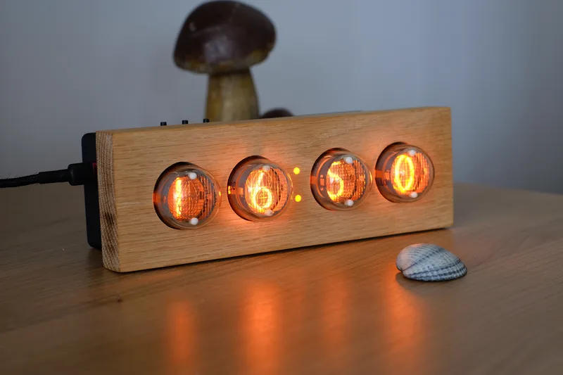
CNIX Nixie Uhr
CNIX is a nixie tube clock that can accept many diffrent nixie tubes with only slight modifications to the tube carrier board.
The motivation was that there are not many clocks out there that let you use almost any nixie tube you like. Most have fixed power supplies, underdesigned driver stages or inflexible microcontrollers. I hope to tackle these problems with an adjustable boost converter PSU, extremely flexible (and electrically protected) driver stages and an open source firmware written with free tools.
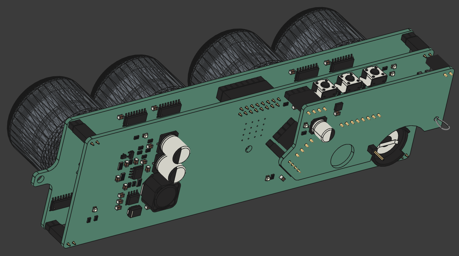
Schematic
The control board consists of 4 parts:
- Power Supply
- Microcontroller
- I/O
- GPIO header
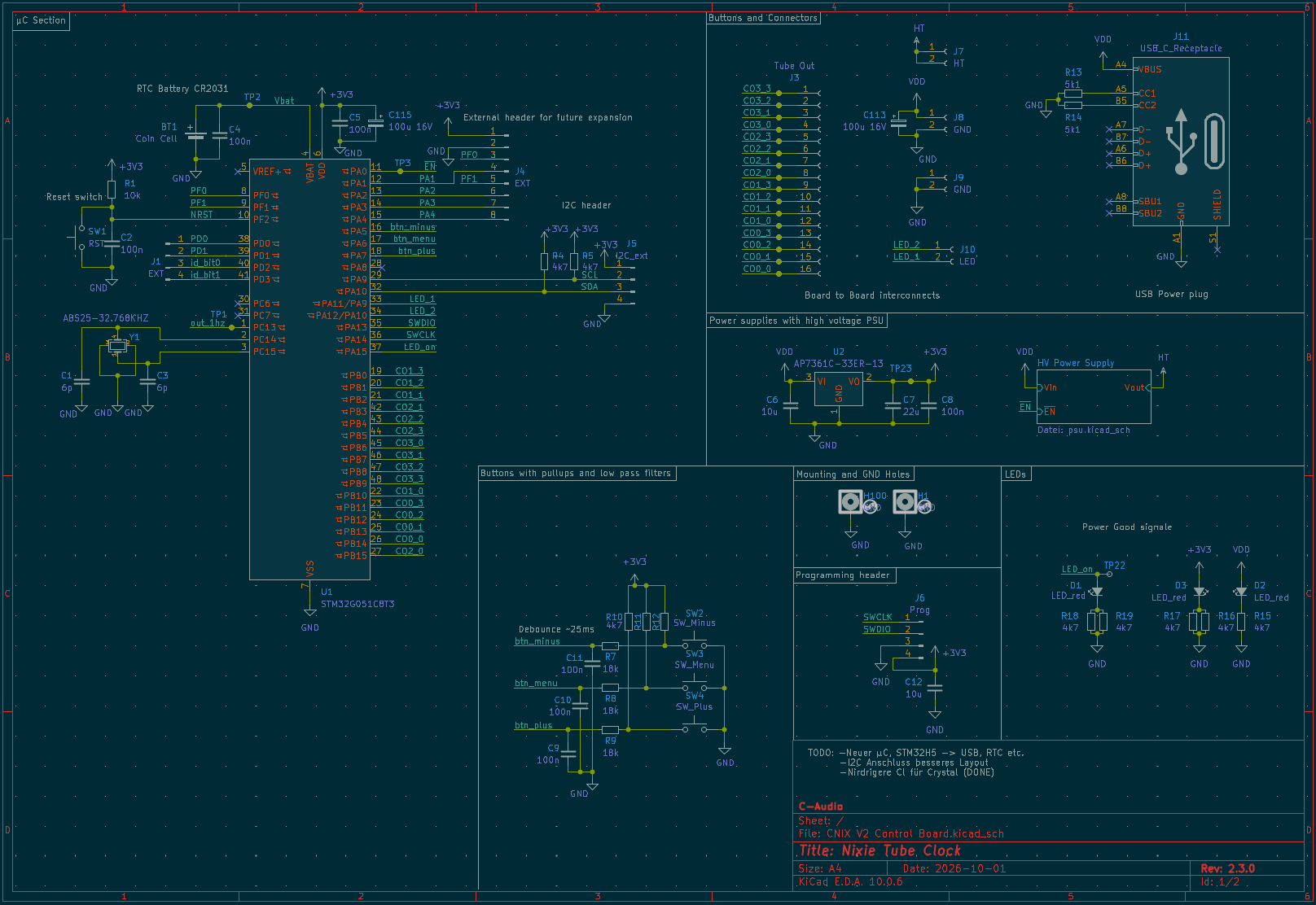
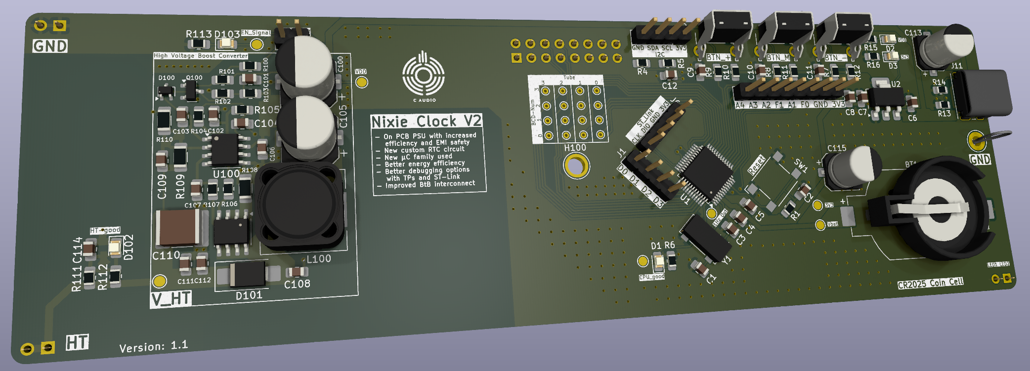
Power comes from a simple USB-C plug configured for 5V 3A max with the 5k1 CC line resistors. I thought about adding a PD controller for higher input voltages, but this would just have added complexity and locked you into more expensive USB PD power supplies.
The µC is a STM32G051, because it has an included RTC with added Vbat pin for an external battery, so that the RTC remembers time even when powered off. The unused GPIOs are broken out to a connector, so that in the future one could add cool stuff like a radio time reciever, a display or wifi. Time is set manually with the push buttons on top.
The PSU is heavily inspired by this site. I highly advise you giving it a read. The article goes in depth with boost converter design and its challanges.
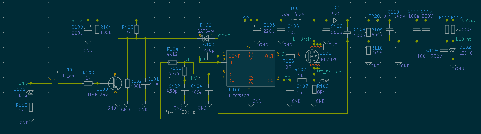
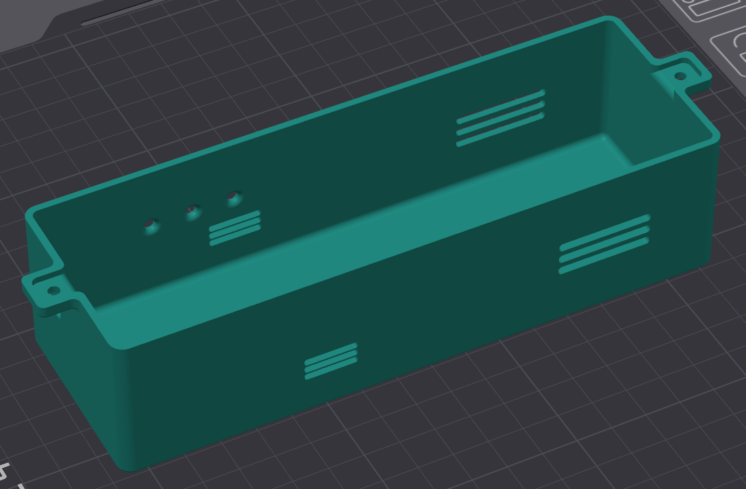
The ht power supply is a DCM boost converter powered by the UCC3803. An active low enable pin is realized via pulling the frequency RC combination low. With normal usage temperature of around 50-60°C are reached by the output transistor and the controller, which is a safe area. The case is designed so that a convection current of air is directed over the power supply at all times. This vent should not be blocked.
The driver consists of 4 CD4028 BCD to Decimal converters and 6 SN75468 high voltage drivers. The SN75468 only work up top 100V, but when using two 48V zener diodes as clamps, the voltage on the torned off digits never reach above 100V and above the startup voltage of the nixies. So win win.
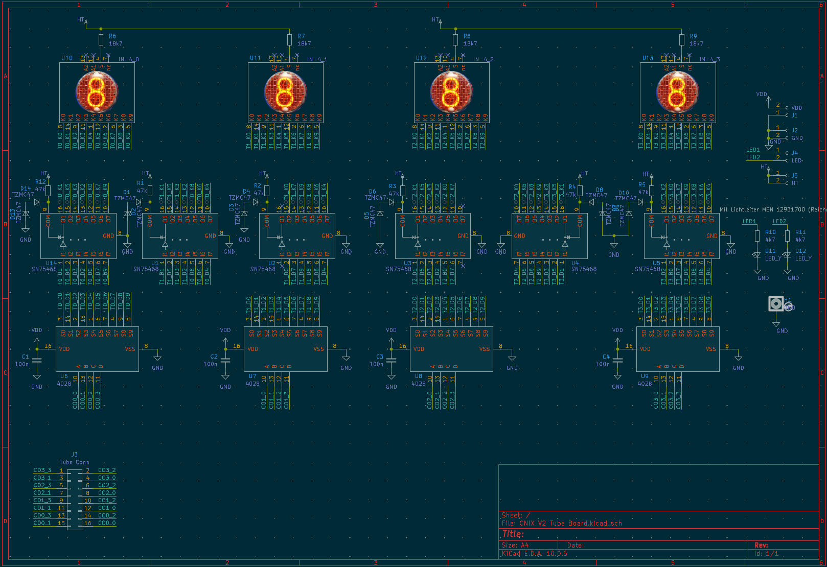
I didn’t use the old high voltage nixie driving shift registers as they are more and more hard to find for a reasonable price. Also i did not use shift registers at all, to simplify programming and wiring. Instead the whole Port B of the STM32 is used as a big 16 bit control register where the numbers are encoded in BCD. This ensures that there can not be 2 turned on digits at the same time in one tube to prevent bugs and damaging the beautiful nixies. Except the decoupling capacitors, diopdes and LEDS, everything is a simple to reflow solder IC, The tube pins have to be assembled manually (by putting them on a tube an inserting it into the holes before soldering it to ensure perfect alignment).
The case is designed in FreeCAD and printed in PLA or PETG. Assembly is a bit of a hassle, but the fit is perfect. You can print a front plate, but i think the clock is vastly more beautiful when paired with a wooden front plate. Drill files for this are within the CAD folder. The holes for the LED front indicators can be filled with a 3mm lightpipe cut to length, to get a beautiful finish. Case, PCB and front plate are screwed together with 15mm M3 wood screws.
Neat features
Adaptability
If you want to use any other nixie (up to around 5mA per tube of HT supply current) just modify the tube board PCB to fit your tubes. The driver, power supply and control logic should all be compatible with any other tube. Of course you have to modify the driving circuit when not using the simple common anode topology.
USB-C support
Use any USB power supply with a minimum current of 1.7A (The startup of the boost converter needs a lot of current) Standard power consumption is around 2W (400mA at 5V) when the boost converter is powered on and around 0.2W (40mA at 5V) when the boost converter is powered down.
Fallback structure
If for some reason you change your mind while setting the start/stop times or the main time, just wait for around a minute. The menu will exit automatically, discard all changes and get back to the main time display.
Date and Sensor display
Press the “plus” or “minus” buttons to cycle through submenus in this order: Main Time display -> Date display -> Sensor Display These have a short timeout time to get back to the main Time menu. The sensor display gets disabled when there is no sensor addon board present.
Automatic daylight saving time (DST)
The clock will calculate DST on its own and set the time correspondingly, even when the DCF77 module is not used.
Turn on/off timers
You can set power on and off times in the clock natively, so that the nixies dont always glow. With this the HT-power supply also gets deactivated to save power and lifespan of the parts. There are two sets of start and stop times set by the buttons on the menu with the lower LED blinking. The order is: Start1 -> Stop1 -> Start2 -> Stop2. If all are set to 0, the start stop automatic gets disabled. The start stop times are saved to a backup register of the µC, so the clock remembers them even when powered off as long as the RTC battery is present.
Peek
When out of the “on” timeframes you can “peek” at the current time for 10s with a press of the menu-button. During these 10s you can jump to all the diffrent menus.
Addon Boards
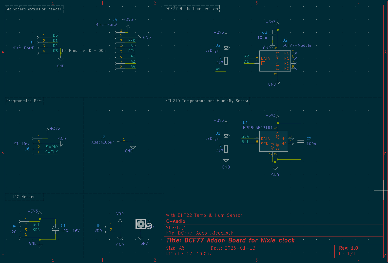
The breakout pins next to the µC can be used for addon boards. Pins D2 and D3 of the µC are used to detect those with an ID system.
| ID | Board |
|---|---|
| 0b11 | No Addon board installed -> defualt |
| 0b00 | DCF77 Addon Board used |
| 0b01 | not yet used |
| 0b10 | not yet used |
Most of the hardware features of the STM32G051 should be mapped to the pins on the breakout. If not you’re out of luck (it’s open source, so just change it). Stuff like the ST-Link programming pins or I2C are broken out on extra headers to simplify future expansion.
DCF77 Addon Board
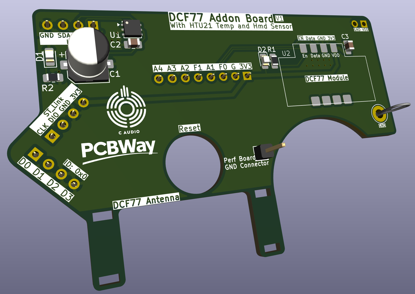 In germany (and most of europe) we have the DCF77 signal pushed out by the radio transmitter near Frankfurt.
This board hosts a cheap module from ebay and a HTU21D temperature and humidity sensor. The driver is already programmed into the Control Board and gets enabled when this addon board is detected.
When a valid time is recieved the manual timeSet menu gets disabled, to prevent fuckery.
It is setup, that every night at 2 an alarm gets triggered by the RTC to recalibrate time. If the time-parity bit is not matched within a 20 minute timeout an attempt counter is incremented, which gets saved to a backup-register inside the RTC. As long as a RTC battery is powering the µC this register is kept even when the power is off.
If the attempt counter reches 3 days without successful calibration against the radio time the manual timeSet menu gets enabled again.
In germany (and most of europe) we have the DCF77 signal pushed out by the radio transmitter near Frankfurt.
This board hosts a cheap module from ebay and a HTU21D temperature and humidity sensor. The driver is already programmed into the Control Board and gets enabled when this addon board is detected.
When a valid time is recieved the manual timeSet menu gets disabled, to prevent fuckery.
It is setup, that every night at 2 an alarm gets triggered by the RTC to recalibrate time. If the time-parity bit is not matched within a 20 minute timeout an attempt counter is incremented, which gets saved to a backup-register inside the RTC. As long as a RTC battery is powering the µC this register is kept even when the power is off.
If the attempt counter reches 3 days without successful calibration against the radio time the manual timeSet menu gets enabled again.
On the DCF77 Addon board there is a single pin to give structural strength to a simple perfboard on the main breakout bus. One can use this in tandem with the A1, A2, A3, A4, F0 and F1 pins.
Ideas for future addon Boards:
- ESP32 addon board to integrate WiFi time synchronisation or HomeAssistant integration
- Other sensors like air quality sensors
- maybe displays?
TODO
- Change to new MCU. STM32H5 for USBC pd -> more efficient boost converter because higher input voltage
- Sleep modes during off times paired with wakeup alarms at start times -> reduce power consumption even more
- Improve the case to simplify assembly
- More tube boards to fit more types of nixies (IN-14 e.G.)
- BOM optimization to reduce number of unique parts
- galvanic isolation between high voltage areas and µC GPIOs